
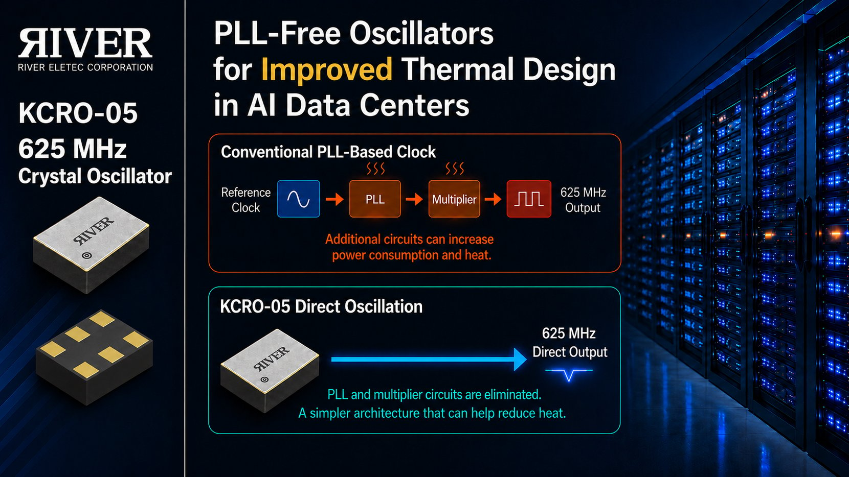
As generative AI continues to gain widespread adoption, power consumption in GPU servers and high-speed optical communication equipment is increasing rapidly, making heat generation and cooling capacity critical design challenges for AI data centers. Although strengthening cooling infrastructure is an effective solution, there are limits to improving efficiency by simply removing heat after it has already been generated.
For this reason, in addition to enhancing cooling systems, reducing heat generation at its source within servers and communication equipment has become an increasingly important design strategy. When communication performance deteriorates, retransmissions and processing delays can prevent GPU resources from being fully utilized, ultimately reducing the overall power efficiency of the system.
Against this backdrop, selecting timing devices based on clock performance and phase jitter has become increasingly important. This article examines the thermal and power challenges facing AI data centers and explains how PLL-free oscillators can contribute to a low-power, low-heat design approach.
Thermal and Power Challenges Are Intensifying in AI Data Centers
As generative AI continues to gain widespread adoption, GPU density in AI data centers is increasing, making power consumption and heat generation increasingly significant design challenges. In particular, as power density per rack continues to rise, conventional air-cooling systems are becoming insufficient for many high-performance deployments.
This section examines the factors driving the growing thermal and power challenges in AI data centers and explains why enhancing cooling infrastructure alone is no longer sufficient to address them.
The Widespread Adoption of Generative AI Is Driving Increases in Power Consumption and Heat Generation
As generative AI continues to gain widespread adoption, power consumption and heat generation in AI data centers are increasing rapidly. A key factor behind this trend is the growing density of GPUs used to support AI training and inference workloads. Deploying large numbers of GPUs within a single rack is becoming the standard architecture, driving rack-level power density far beyond that of conventional data centers.
In addition to the intensive computational demands of AI training, inference workloads are increasingly running continuously, resulting in sustained heat generation. Looking ahead, rack designs with power densities of 200 kW or more are already under discussion, making thermal design an even greater engineering challenge.
The increase in heat generation extends well beyond the servers themselves. It affects power distribution systems, cooling infrastructure, cabling, and airflow management within equipment enclosures. As a result, thermal management in AI data centers is evolving from a chip-level concern into a facility-wide design challenge.
Cooling Infrastructure Alone Is No Longer Sufficient
In AI data centers, addressing thermal challenges through increased cooling capacity alone is becoming increasingly difficult. Conventional air-cooling systems have long been widely used, but as AI racks become more densely integrated, they are beginning to approach the limits of their cooling capabilities.
In recent years, liquid cooling has attracted growing attention, and real-world deployments are becoming more common. However, challenges related to capital investment and operational complexity mean that it has yet to become the standard solution across all facilities. Although cooling technologies continue to advance, relying solely on cooling infrastructure is no longer sufficient to address the industry's growing thermal challenges.
At the same time, data center operators are under increasing pressure to improve Power Usage Effectiveness (PUE). As a result, improving cooling efficiency alone is no longer enough. Reducing heat generation at its source has become an equally important design consideration.
In the AI era, effective thermal design is no longer just about removing heat after it is generated. It also requires designing systems that inherently generate less heat in the first place.
Why Clock Performance Requirements Are Increasing in the 1.6T Optical Communication Era
The performance of AI data centers depends on more than just GPUs. High-speed communication between GPUs is equally critical. As communication speeds continue to evolve from 800G to 1.6T—and eventually to 3.2T—the performance requirements for clock sources are becoming increasingly stringent.
This section examines the impact of jitter and phase noise in high-speed optical communication and explains the clock performance required to support next-generation communication systems.
The Growing Impact of Jitter and Phase Noise in High-Speed Communication
In high-speed communication systems, clock performance plays a critical role in maintaining communication stability. As communication speeds continue to increase, even slight variations in clock timing can have a significant impact on signal integrity.
Jitter refers to variations in signal timing, while phase noise describes short-term fluctuations in the frequency domain. As phase noise increases, the timing of signal transitions becomes less stable, potentially leading to higher Bit Error Rates (BER).
In particular, for high-speed interfaces, the performance of the clock source is a key factor influencing the overall performance of the communication link. As timing margins become increasingly narrow, communication systems become more susceptible to temperature fluctuations, manufacturing tolerances, and long-term aging effects.
In 1.6T-class high-speed optical communication, it is no longer sufficient for a clock source to simply meet basic operating requirements. It must deliver stable clock performance that maintains reliable communication across a wide range of operating conditions, making it a critical design requirement for next-generation communication systems.
Increasing Demands on Clock Performance in the Transition to the 3.2T Era
As communication speeds continue to increase, performance requirements for clock sources are becoming even more demanding. High-precision clock sources are already a fundamental requirement for 1.6T-class optical communication systems, and as the industry moves toward 3.2T, the allowable timing margin will become even narrower.
The challenge extends beyond achieving higher operating frequencies. Next-generation clock sources must combine ultra-low-jitter performance with excellent frequency stability, while also minimizing power consumption and heat generation. In equipment designed for next-generation 800G and 1.6T optical communication, the importance of ultra-low-jitter reference clocks continues to grow, and the demand for higher clock performance will increase in step with communication speeds.
Looking ahead, the adoption of 3.2T optical communication and co-packaged optics (CPO) is expected to place even greater demands on integration density and thermal design. As a result, the clock source can no longer be viewed simply as a frequency-generation component. It must be regarded as a critical element that supports both communication performance and overall system efficiency.
New Design Challenges Introduced by Noise Mitigation
In high-speed communication systems, a variety of noise mitigation techniques are employed to maintain signal integrity. However, adding noise-suppression circuitry can introduce new design challenges, including increased board space requirements, higher power consumption, and greater heat generation.
This section examines the role of noise mitigation circuits and the engineering trade-offs associated with incorporating them into high-speed communication systems.
The Role of PLLs, Jitter Cleaners, and Compensation Circuits
High-speed communication systems employ multiple types of noise mitigation circuitry to maintain clock performance. As communication speeds continue to increase, timing margins become increasingly narrow, meaning that even small amounts of jitter or phase noise can degrade signal integrity and overall communication performance.
The primary functions of these noise mitigation circuits are summarized below.
|
Circuit |
Primary Function |
|
PLL (Phase-Locked Loop) |
Frequency stabilization and high-frequency clock generation |
|
Jitter Cleaner |
Improves signal integrity by reducing jitter |
|
Compensation Circuit |
Compensates for temperature variations and manufacturing or assembly tolerances |
As communication speeds continue to increase, the performance requirements placed on clock sources become increasingly stringent. In particular, in 1.6T-class optical communication systems, even slight timing variations can increase the Bit Error Rate (BER) and degrade communication performance.
For this reason, clock design must address more than just high-frequency clock generation. It must also incorporate measures to minimize jitter and maintain stable operation across temperature variations. In high-speed communication equipment, these circuits work together to ensure reliable communication performance and preserve system timing margin.
Increasing Component Count, Heat Generation, and Board Space Requirements
Although noise mitigation circuits are highly effective at improving communication performance, they also introduce additional design challenges. Adding PLLs, jitter cleaners, and compensation circuits increases the number of ICs and supporting components, resulting in greater board space requirements.
In optical modules and AI data center accelerator cards, where high-density integration is essential, the additional circuitry can significantly reduce layout flexibility. Furthermore, the use of more active circuits generally increases the overall power consumption of the system.
Higher power consumption inevitably leads to greater heat generation. As localized hot spots develop, thermal design becomes more complex, often increasing both the cost and engineering effort required for effective thermal management.
When designing high-speed communication systems, optimizing signal integrity alone is no longer sufficient. Designers must also balance board space requirements, power consumption, and thermal performance to achieve an efficient and reliable system design.
How Clock Performance Influences Overall System Efficiency
A decline in clock performance affects far more than communication errors alone. In large-scale parallel processing environments such as AI training, retransmissions and communication delays can lead to underutilized GPU resources, ultimately reducing the overall power efficiency of the system.
This section examines how ultra-low-jitter clock performance contributes to improved communication performance and higher GPU utilization in AI data centers.
Why Ultra-Low Jitter Improves Overall System Efficiency
AI training relies on thousands to tens of thousands of GPUs working together in parallel. As a result, overall system performance depends not only on the processing power of individual GPUs, but also on the performance of the high-speed communication that connects them.
As clock jitter and phase noise increase, the timing margin available for signal detection at the receiver becomes narrower, potentially leading to a higher Bit Error Rate (BER). As communication errors increase, retransmissions become more frequent, reducing effective data throughput. In addition, as more GPUs spend time waiting for data transfers to complete, overall GPU utilization declines, preventing available computing resources from being fully utilized.
In large-scale AI data centers, the cumulative effect of these seemingly small inefficiencies can significantly impact both system throughput and power efficiency. In other words, an ultra-low-jitter clock source is more than just a component that supports communication performance—it is also a key technology for maximizing GPU utilization and improving overall system efficiency.
A Design Philosophy That Reduces Noise at the Clock Generation Stage
In high-speed communication systems, it is common practice to compensate for noise using PLLs, jitter cleaners, and other signal-conditioning circuits. However, as communication speeds continue to increase, the additional board space, power consumption, and heat generation associated with these compensation circuits are becoming increasingly difficult to ignore.
As an alternative approach to maintaining communication performance, growing attention is being given to design philosophies that reduce noise at the clock generation stage, rather than relying solely on downstream compensation. By lowering the phase noise of the oscillator itself, it becomes easier to minimize BER degradation and reduce retransmissions, which can also help reduce GPU idle time caused by communication delays.
Furthermore, when the clock source provides sufficiently high performance, it may be possible to reduce the number of compensation circuits required downstream. A simpler circuit architecture can help reduce board space requirements, power consumption, and heat generation, contributing to a more efficient overall system design.
In AI data centers, reducing noise at the clock generation stage is emerging as an important design strategy for simultaneously improving communication performance and reducing the burden on thermal management.
PLL-Free Clock Design Enabled by the KCRO-05
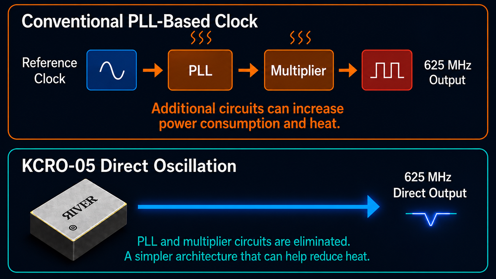
The KCRO-05 is a PLL-free crystal oscillator that adopts a Direct Oscillation architecture, generating a 625 MHz output directly without relying on a PLL or frequency multiplier circuits. By minimizing noise at the clock generation stage, it enables both ultra-low-jitter performance and a simplified circuit architecture.
This section explains the design characteristics of Direct Oscillation and the advantages it offers for thermal management and next-generation high-speed communication systems.
A PLL-Free Architecture That Directly Generates a 625 MHz Clock
One of the key features of the KCRO-05 is its Direct Oscillation architecture, which generates a 625 MHz clock signal directly. In conventional high-speed communication systems, the required operating frequency is typically generated by multiplying a lower-frequency reference clock using a PLL or other frequency multiplier circuits.
By contrast, the KCRO-05 outputs a 625 MHz clock directly from the oscillator itself, eliminating the need for a PLL or frequency multiplier circuits. This simplified clock generation path makes the system less susceptible to the jitter and phase noise that can be introduced during the frequency multiplication process.
Another key advantage is that the performance of the clock source is delivered directly to the system without intermediate frequency conversion. As performance requirements become increasingly stringent in 800G and 1.6T-class optical communication systems, minimizing potential noise sources from the clock generation stage has become an increasingly important design strategy.
Enabling a Simpler Circuit Architecture
One of the key advantages of a PLL-free architecture is its potential to simplify the overall circuit design. By reducing the amount of circuitry required for clock generation, it can help minimize board space requirements while also reducing design complexity.
In conventional architectures, PLLs, frequency multiplier circuits, and additional circuitry for jitter reduction and phase compensation are often required. By contrast, when a high-frequency clock can be generated directly—as with the KCRO-05—it may be possible to simplify the downstream clocking architecture and reduce the need for additional signal-conditioning circuits.
Reducing the number of components can also help minimize PCB footprint, providing a significant advantage in optical modules and AI data center accelerator cards, where high-density integration is essential.
A simpler circuit architecture may also reduce the number of circuits that require design verification and performance evaluation, helping to shorten both development time and system optimization efforts.
The Thermal Management Advantages of a PLL-Free Architecture
In AI data centers, thermal design is no longer just about how efficiently heat can be removed. It also requires reducing heat generation at its source. A PLL-free architecture represents one approach that aligns with this design philosophy.
Because the KCRO-05 does not rely on a PLL or frequency multiplier circuits, it enables a simpler clock generation architecture. By generating a high-frequency clock directly, it may also reduce the need for downstream jitter cleaners and compensation circuits, helping to minimize board space requirements, power consumption, and heat generation around the clocking circuitry.
Improving clock performance can also help reduce communication errors and retransmissions, potentially improving GPU utilization by minimizing idle time caused by communication delays. As a result, evaluating a clock source should involve more than considering the oscillator's own power consumption. It should also take into account its contribution to overall system efficiency through improved communication performance.
The KCRO-05 also features a compact 2520-size package, making it well suited for high-density integration. By helping maximize the use of limited PCB space, it provides additional design flexibility for optical modules and AI data center equipment, supporting further miniaturization and higher integration densities.
Clock Performance Enabled by KoT cut® and OPAW® Technologies
The KCRO-05's ultra-low-jitter performance and high-temperature stability are made possible by River Eletec's proprietary KoT cut® and OPAW® technologies. Delivering stable clock performance in high-temperature environments requires not only advanced oscillation technology but also optimized crystal characteristics.
This section introduces the underlying technologies that enable PLL-free high-frequency oscillation.
High-Temperature Stability Enabled by KoT cut®
In high-speed optical communication equipment and AI servers, temperature fluctuations caused by heat generation can affect clock performance. As a result, not only the oscillator circuitry but also the thermal characteristics of the crystal resonator itself have become important design considerations.
KoT cut® is River Eletec's proprietary crystal-cut technology, developed to significantly reduce frequency variation caused by temperature changes compared with conventional AT-cut crystals. By improving the crystal's temperature characteristics, KoT cut® helps maintain stable frequency performance even as the operating environment changes.
Within AI servers and optical transceivers, sustained high workloads can result in operating temperatures exceeding 80°C. Under these conditions, suppressing frequency variation contributes to maintaining stable communication performance.
For clock sources used in high-speed optical communication, ultra-low-jitter performance alone is no longer sufficient. Maintaining stable performance under high-temperature operating conditions has become an equally important design requirement.
OPAW® Technology Enables PLL-Free High-Frequency Oscillation
High-frequency clocks are traditionally generated by increasing the frequency of a lower-frequency reference clock using a PLL or frequency multiplier circuits. However, as additional circuitry is introduced, its impact on noise, power consumption, and overall system complexity must also be taken into consideration.
OPAW® is River Eletec's proprietary technology for directly generating high-frequency signals from a crystal resonator. By enabling fundamental-mode oscillation in the 500–1000 MHz range without relying on a PLL or frequency multiplier circuits, it allows for a simpler clock generation architecture.
Another key advantage of this architecture is that it minimizes the influence of jitter and phase noise that can be introduced during the clock generation process. As a result, OPAW® contributes to the ultra-low-noise and ultra-low-jitter performance required for high-speed optical communication systems.
Together with KoT cut®, OPAW® serves as one of the core technologies that enables PLL-free high-frequency clock design.
Specifications That Ensure Stable Operation in High-Temperature Environments
For timing devices used in high-speed optical communication systems, achieving both ultra-low-jitter performance and thermal stability is essential. As communication speeds continue to increase, even slight timing variations can affect overall system performance. As a result, timing devices must be capable of maintaining stable performance even under elevated operating temperatures.
The key specifications of the KCRO-05 are shown below.
|
Parameter |
KCRO-05 Specification |
|
RMS Phase Jitter |
Typ. 12 fs |
|
Maximum Phase Jitter |
Max. 20 fs |
|
Operating Temperature |
−40°C to +105°C |
|
Storage Temperature |
−40°C to +125°C |
Within AI servers and optical transceivers, operating temperatures can fluctuate significantly under sustained high workloads. In these environments, the thermal stability and jitter performance of the clock source play an important role in maintaining stable communication performance.
For timing devices used in high-speed communication equipment, ultra-low-jitter performance alone is not enough. Reliable operation across a wide operating temperature range is equally critical. When evaluating a clock source, engineers should consider not only its contribution to communication performance, but also its ability to maintain stable operation under demanding thermal conditions.

Key Considerations When Selecting Timing Devices for Next-Generation Communication Systems
As the industry advances from 1.6T to 3.2T and ultimately toward co-packaged optics (CPO), the performance requirements for timing devices continue to become more demanding. In addition to ultra-low-jitter performance, factors such as compact form factors, high-temperature stability, and power and thermal performance under real-world operating conditions have become increasingly important evaluation criteria.
This final section summarizes the key considerations for selecting clock sources that are well positioned to support the next generation of high-speed optical communication systems.
Supporting High-Density Integration with a 2520 Package
In high-speed optical communication systems, achieving higher integration density has become just as important as improving communication performance. As the industry advances from 1.6T to 3.2T, the number of components integrated within optical modules continues to increase, making efficient use of limited PCB space an increasingly important design consideration.
The KCRO-05 is housed in a compact 2520 package measuring 2.5 × 2.0 mm.
|
Package |
Size |
|
Standard 3225 Package |
3.2 × 2.5 mm |
|
KCRO-05 (2520 Package) |
2.5 × 2.0 mm |
Compared with a standard 3225 package, the 2520 package reduces both PCB footprint and package volume by approximately 40%, providing greater layout flexibility in high-density integration environments such as optical transceivers.
In addition to its compact size, the KCRO-05 maintains the ultra-low phase noise and ultra-low-jitter performance required for 625 MHz operation. As co-packaged optics (CPO) and 3.2T-class communication systems continue to evolve, timing devices that combine compact form factors with exceptional clock performance will become increasingly important for maximizing performance within highly space-constrained designs.
Evaluate Power Consumption and Thermal Performance at the Intended Operating Frequency
When evaluating timing devices, it is important to look beyond datasheet specifications and assess performance under the actual operating frequency of the target application. In high-speed communication systems, current consumption and thermal characteristics can vary depending on the operating frequency.
For example, excellent performance at 156.25 MHz does not necessarily indicate the same characteristics at 625 MHz. Unless the device is evaluated under conditions that closely match its intended operating frequency, the accuracy of thermal design and power budgeting may be affected.
In AI servers and optical transceivers, even small differences in power consumption can influence the overall thermal profile of the system. For this reason, selecting a timing device requires evaluating current consumption and thermal characteristics at the intended operating frequency to ensure that its performance meets the demands of real-world operating conditions.
Greater Design Margin Can Help Reduce Development Effort
For next-generation communication systems, improving performance is only part of the challenge. Maintaining development efficiency is equally important. In particular, for ultra-high-speed communication systems beyond 1.6T, it is difficult to accurately predict every source of noise using simulations or prototype test boards alone.
If insufficient jitter margin is discovered during final validation of fully assembled hardware, significant rework may be required, including PCB redesigns and component requalification. Such issues can have a major impact on project schedules. For this reason, selecting timing devices that provide sufficient jitter margin and design margin from the outset has become an important consideration.
A clock source with ample performance margin can help maintain stable communication performance even under the unpredictable conditions encountered in real-world systems. This, in turn, can reduce the time and effort required for debugging and system optimization. Designing with sufficient margin is therefore more than simply pursuing higher performance—it is a strategic approach to reducing development risk and helping projects stay on schedule.
Ultimately, this approach can contribute to shorter development cycles, more stable product quality, and lower overall development effort.
Selecting Clock Sources for the 3.2T Era and Co-Packaged Optics
As communication speeds advance from 1.6T to 3.2T, the performance requirements for clock sources will become even more demanding. In addition to ultra-low-jitter performance, key evaluation criteria will include high-temperature stability, low power consumption, and compact form factors.
In particular, as co-packaged optics (CPO) moves toward broader adoption, the close integration of ASICs and optical engines is expected to place even greater constraints on thermal management and available PCB space. In these high-density integration environments, the PCB footprint and power consumption of timing devices become increasingly important design considerations.
For next-generation communication systems, designers must strike a balance between maintaining communication performance and achieving practical thermal and mechanical designs. When selecting a clock source, it is therefore important to consider not only current performance requirements but also whether the device provides sufficient design margin to support future system generations.
Conclusion: Effective Thermal Management in AI Data Centers Begins with Clock Source Selection
Effective thermal management in AI data centers requires more than simply increasing cooling capacity. It also demands a design approach that reduces heat generation at its source. As communication performance deteriorates, retransmissions and communication delays can reduce GPU utilization, ultimately affecting the overall power efficiency of the system.
As the industry progresses from 1.6T to 3.2T and ultimately toward co-packaged optics (CPO), timing devices will be expected to deliver more than ultra-low-jitter performance. High-temperature stability, compact form factors, and optimized power and thermal performance under real-world operating conditions will become equally important design considerations. Rather than relying solely on more advanced cooling technologies, future system designs will increasingly benefit from approaches that reduce heat generation at its source while improving overall system efficiency through enhanced communication performance.
The KCRO-05 combines PLL-free Direct Oscillation, KoT cut®, and OPAW® technologies to deliver the clock performance required for next-generation communication systems. At the same time, it represents a compelling option for reducing the complexity of thermal management through a simplified clock architecture and high-performance clock source.
